- 您现在的位置:买卖IC网 > Sheet目录1997 > ICS8430S07AKILF (IDT, Integrated Device Technology Inc)IC CLK GENERATOR PLL 32VFQFN
ICS8430S07AKI REVISION A SEPTEMBER 3, 2009
12
2009 Integrated Device Technology, Inc.
ICS8430S07I Data Sheet
CLOCK GENERATOR FOR CAVIUM PROCESSORS
Parameter Measurement Information, continued
LVCMOS Output Duty Cycle/Pulse Width/Period
LVPECL Output Duty Cycle/Pulse Width/Period
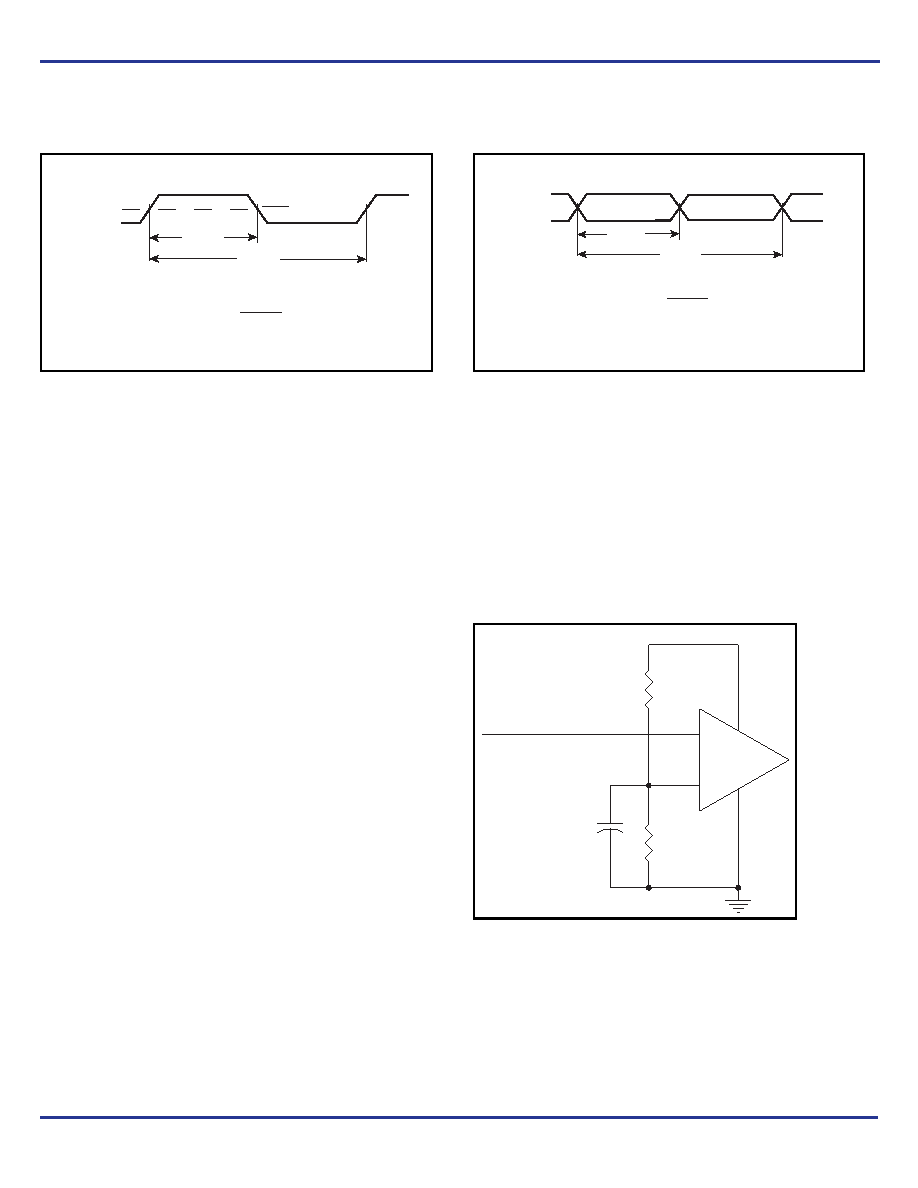
Application Information
Wiring the Differential Input to Accept Single-Ended Levels
Figure 1 shows how the differential input can be wired to accept
single-ended levels. The reference voltage V_REF = VDD/2 is
generated by the bias resistors R1, R2 and C1. This bias circuit
should be located as close as possible to the input pin. The ratio of
R1 and R2 might need to be adjusted to position the V_REF in the
center of the input voltage swing. For example, if the input clock swing
is only 2.5V and VDD = 3.3V, V_REF should be 1.25V and R2/R1 =
0.609.
Figure 1. Single-Ended Signal Driving Differential Input
t
PERIOD
t
PW
t
PERIOD
odc =
V
DDOX
2
x 100%
t
PW
QB:QD,
QREF[0:2]
t
PW
t
PERIOD
t
PW
t
PERIOD
odc =
x 100%
QA
nQA
V_REF
Single Ended Clock Input
VDD
CLK
nCLK
R1
1K
C1
0.1u
R2
1K
发布紧急采购,3分钟左右您将得到回复。
相关PDF资料
ICS8430S10BYI-02LF
IC CLK GENERATOR PLL 48TQFP
ICS84314AY-02LFT
IC SYNTHESIZER 700MHZ 32-LQFP
ICS843156AKILF
IC CLK GENERATOR 32VFQFP
ICS843156AKLF
IC CLK GENERATOR 32VFQFP
ICS843202AYILF
IC SYNTHESIZER 680MHZ 32-LQFP
ICS843204AGILF
IC SYNTHESIZER LVPECL 48-TSSOP
ICS84320AY-01LN
IC SYNTHESIZER GP LVPECL 32-LQFP
ICS84320AYI-01LF
IC FREQ SYNTHESIZER 32TQFP
相关代理商/技术参数
ICS8430S07AKILFT
功能描述:IC CLK GENERATOR PLL 32VFQFN RoHS:是 类别:集成电路 (IC) >> 时钟/计时 - 专用 系列:- 标准包装:1,500 系列:- 类型:时钟缓冲器/驱动器 PLL:是 主要目的:- 输入:- 输出:- 电路数:- 比率 - 输入:输出:- 差分 - 输入:输出:- 频率 - 最大:- 电源电压:3.3V 工作温度:0°C ~ 70°C 安装类型:表面贴装 封装/外壳:28-SSOP(0.209",5.30mm 宽) 供应商设备封装:28-SSOP 包装:带卷 (TR) 其它名称:93786AFT
ICS8430S07I
制造商:IDT 制造商全称:Integrated Device Technology 功能描述:Clock Generator for Cavium Processors
ICS8430S10AYILF
功能描述:IC CLK GENERATOR PLL 48TQFP RoHS:是 类别:集成电路 (IC) >> 时钟/计时 - 专用 系列:- 标准包装:1,500 系列:- 类型:时钟缓冲器/驱动器 PLL:是 主要目的:- 输入:- 输出:- 电路数:- 比率 - 输入:输出:- 差分 - 输入:输出:- 频率 - 最大:- 电源电压:3.3V 工作温度:0°C ~ 70°C 安装类型:表面贴装 封装/外壳:28-SSOP(0.209",5.30mm 宽) 供应商设备封装:28-SSOP 包装:带卷 (TR) 其它名称:93786AFT
ICS8430S10AYILFT
功能描述:IC CLK GENERATOR PLL 48TQFP RoHS:是 类别:集成电路 (IC) >> 时钟/计时 - 专用 系列:- 标准包装:1,500 系列:- 类型:时钟缓冲器/驱动器 PLL:是 主要目的:- 输入:- 输出:- 电路数:- 比率 - 输入:输出:- 差分 - 输入:输出:- 频率 - 最大:- 电源电压:3.3V 工作温度:0°C ~ 70°C 安装类型:表面贴装 封装/外壳:28-SSOP(0.209",5.30mm 宽) 供应商设备封装:28-SSOP 包装:带卷 (TR) 其它名称:93786AFT
ICS8430S10BYI-02LF
功能描述:IC CLK GENERATOR PLL 48TQFP RoHS:是 类别:集成电路 (IC) >> 时钟/计时 - 专用 系列:- 标准包装:1,500 系列:- 类型:时钟缓冲器/驱动器 PLL:是 主要目的:- 输入:- 输出:- 电路数:- 比率 - 输入:输出:- 差分 - 输入:输出:- 频率 - 最大:- 电源电压:3.3V 工作温度:0°C ~ 70°C 安装类型:表面贴装 封装/外壳:28-SSOP(0.209",5.30mm 宽) 供应商设备封装:28-SSOP 包装:带卷 (TR) 其它名称:93786AFT
ICS8430S10BYI-02LFT
功能描述:IC CLK GENERATOR PLL 48TQFP RoHS:是 类别:集成电路 (IC) >> 时钟/计时 - 专用 系列:- 标准包装:1,500 系列:- 类型:时钟缓冲器/驱动器 PLL:是 主要目的:- 输入:- 输出:- 电路数:- 比率 - 输入:输出:- 差分 - 输入:输出:- 频率 - 最大:- 电源电压:3.3V 工作温度:0°C ~ 70°C 安装类型:表面贴装 封装/外壳:28-SSOP(0.209",5.30mm 宽) 供应商设备封装:28-SSOP 包装:带卷 (TR) 其它名称:93786AFT
ICS8430S10I-03
制造商:IDT 制造商全称:Integrated Device Technology 功能描述:Clock Generator for Cavium Processors
ICS8431-01
制造商:ICS 制造商全称:ICS 功能描述:200MHZ, LOW JITTER, LVPECL FREQUENCY SYNTHESIZER